
PCB Capabilities Demonstration


Schematic and board layout in Altium
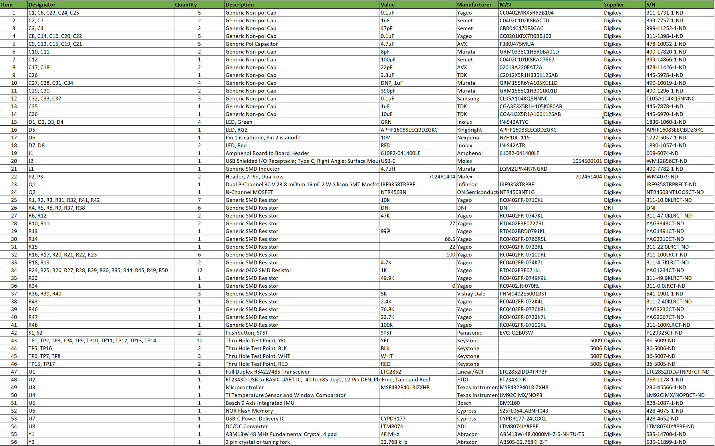
Because all of my previous work is proprietary, I wanted to build a small printed circuit board paid for out of pocket to build my design portfolio. The board is currently being manufactured and assembled and I will be adding pictures of the finished board when it’s completed. I will be developing software to exercise all the features of the board and the MSP432 microcontroller, placing the code in a public Github repository.
Board Level block diagram
This circuit board is a simple 4-layer PCB (2 signal and 2 power layers) with an MSP432 microcontroller, USB-C power delivery, FTDI USB to UART converter, IMU, temperature sensor, DC/DC switching converter, and flash memory chip. The PCB has a external connections for JTAG and an external UART through standard 0.1" headers as well as the ability to plug into a daughter board and provide SPI, I2C, and GPIO interfaces. The board can be powered via USB-C, 0.1" headers, or through the daughter board connection. There are two push buttons, one for reset and one for user interface, on the board as well as debug LEDs and an RGB LED connected to the MSP432's PWMs.


0.5mm pitch Bga
I selected a BGA package for the MSP432 as a better demonstration of capability. Other packages are cheaper because they don’t drive challenging requirements during manufacturing. This 0.5mm pitch BGA drives a 3.2mil trace and space and a 5 mil minimum drill size which increases the cost and complexity of manufacturing the board. Small pitch BGA packages are also used for FPGA and DDR packages because of the pin density required.
This BGA is broken out using dogboned vias as opposed to using vias in the pads of the BGA. The vias are tented(covered by soldermask) underneath the BGA to prevent solder flowing from the ball of the package into the via that it’s connected to. The smallest decoupling capacitors are placed on the bottom of the board directly behind the power and ground pins of the microcontroller. Because these capacitors are in a 0201 package, they can fit in between the BGA pitch and via fanout without a via into a pad of a capacitor footprint.